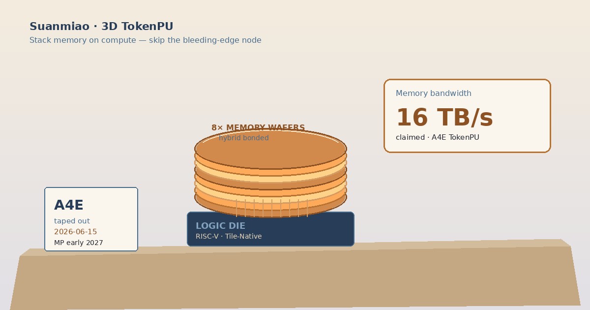
Large-model inference is often bandwidth-bound before it is FLOPS-bound: parameters shuttle between memory and compute, and every millimeter of hop costs latency, energy, and dollars. Suanmiao’s answer — reported across Caixin, 21st Century Business Herald, Xin Dongxi / QQ, and Pedaily — is to treat that hop as the product: stack the memory warehouse on top of the compute floor with 3D hybrid bonding, and run on relatively mature domestic process nodes instead of chasing the latest foundry node that Chinese startups cannot freely buy.
Press coverage of the latest rounds (led by Beijing municipal- and district-level platforms including E-Town Capital / 亦庄国投) puts cumulative fundraising near ¥20亿 in about a year. Caixin-linked reporting and Xin Dongxi put post-money valuation around ¥12 billion. Treat valuation as press reporting, not an audited 409A.
A4E: eight wafers, RISC-V, Tile-Native
Company materials and Xin Dongxi coverage say first-gen 3D TokenPU part A4E taped out on June 15, 2026: proprietary RISC-V plus in-house IP; eight memory wafers vertically hybrid-bonded onto a compute logic wafer via through-silicon vias and micron-scale interconnects; target memory-access bandwidth of 16 TB/s. The architecture pitch is Tile-Native — tiles as the unit of data movement, storage, and compute so data can move once and be reused — with a software toolchain described as compatible with open ecosystems such as LLVM and Triton.
That software story matters for overseas engineers more than the fundraising slide. A RISC-V + LLVM/Triton path is at least legible next to closed CUDA stacks; whether Suanmiao’s compiler actually tracks upstream Triton and ships useful kernels is an empirical question for whenever silicon and SDKs leave the partner lab.
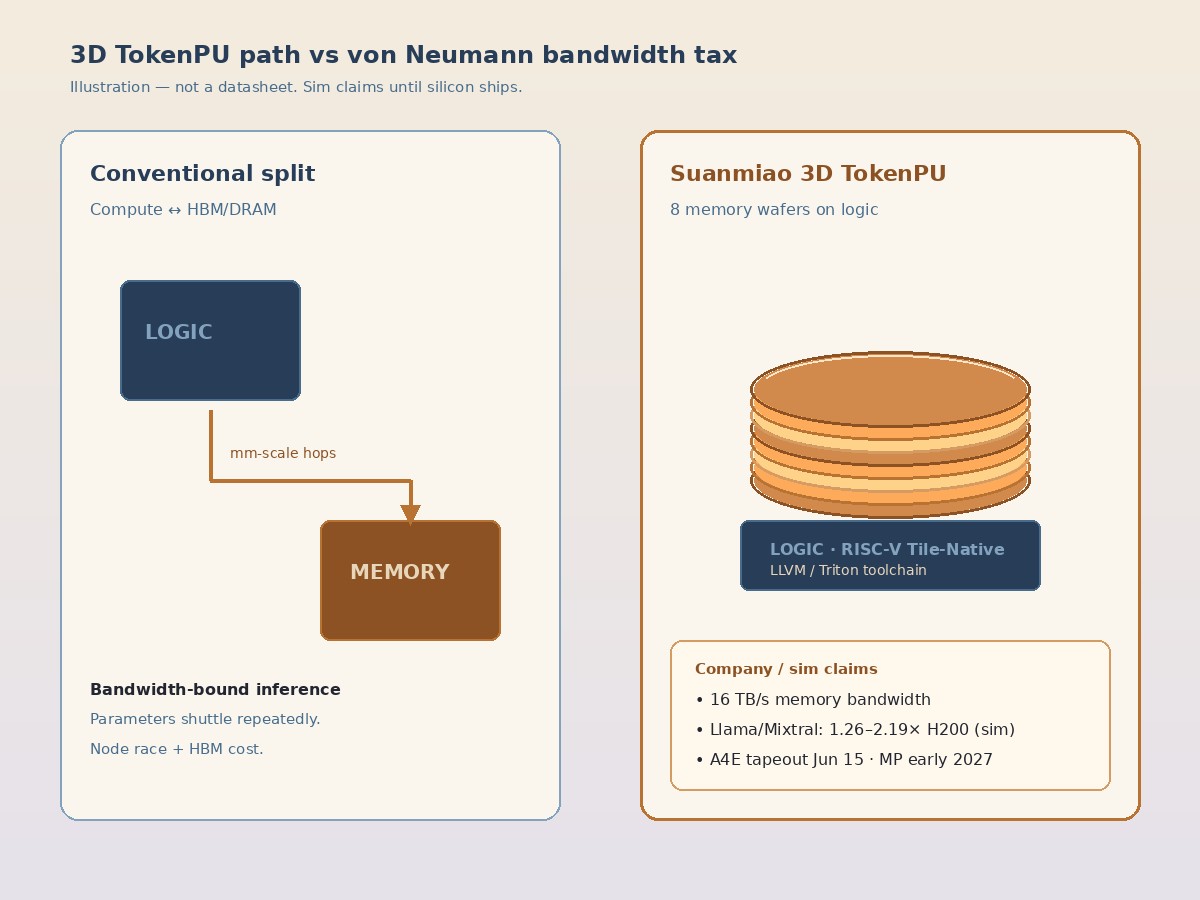
Illustration: von Neumann bandwidth tax vs stacked TokenPU path. Llama/Mixtral vs H200 figures are simulation, not measured silicon.
The H200-multiple line — read the footnote
Xin Dongxi / Jiwei reporting attributes to company simulation data: when running mainstream open models such as Llama and Mixtral, A4E inference throughput is claimed at roughly 1.26× to 2.19× an NVIDIA H200. That is the headline number making the rounds in Chinese tech media. It is also the number that should stay in quotes until independent silicon benches exist. Simulation ≠ shipping silicon; yield, thermal, packaging, and real memory timing all sit between June tapeout and a rack that overseas buyers can rent.
Roadmap language in the same coverage: mass production targeted for early 2027; second-gen A4S architecture defined with a planned Q1 2027 tapeout and company goals of roughly a performance doubling (optimized path described as up to ~2–3×). Label those as company targets.
Not as a buyable accelerator today. A4E is post-tapeout / pre–mass-production per Chinese press; the usable overseas watch-list is early-2027 silicon delivery, partner access with domestic large-model labs, and whether an LLVM/Triton-facing SDK ever appears outside China-only channels. Investors are heavily state-backed (E-Town and other Beijing platforms alongside private funds). Expect China supply-chain packaging and a China-first customer set until someone publishes an international buy or cloud SKU.
Who is building it
Suanmiao was founded in November 2022 and is headquartered in Beijing’s Daxing district. English coverage and Xin Dongxi sketch a Loongson / Chinese Academy of Sciences pedigree: founder Wang Fuquan (汪福全) with CAS Acoustics and ICT / Hu Weiwu lineage; CTO Liu Ming with ~15 years on Loongson semiconductor R&D and prior 3D-stack chip landings; other named leads spanning algorithms, AI, and systems software (including open-source MiniGUI / HVML work). The company claims the core team has roughly seven years of 3D IC experience, earlier wafer-on-wafer hybrid-bonding supply-chain work in mainland China, and prior volume on related 3D products (press cites >10,000 3D IC wafers and >¥1.2B cumulative related revenue from that lineage). Those are company/press figures — useful as pedigree, not as proof that A4E yield will be easy.
Honest caveats
- Simulation only — 1.26–2.19× H200 on Llama/Mixtral is attributed simulation, not third-party silicon measurement.
- Not shipping — A4E taped out June 15, 2026; mass production is a 2027 target, not a SKU you can PO today.
- Bandwidth claims — 16 TB/s is a company target/claim for the stacked design.
- Capital mix — latest rounds heavily municipal/district state-backed; China supply-chain and policy coupling is part of the story.
- Competitive field — Chinese press notes a crowded 3D-stack startup wave and Big Fund / hybrid-bond interest; Suanmiao is one data point, not the only stack.
For overseas inference engineers, the interesting claim is architectural: if memory bandwidth is the bottleneck and advanced nodes are gated, hybrid-bonded memory-on-logic plus an open-ish compiler surface is a coherent bet. The boring, correct next step is to wait for early-2027 silicon numbers — and to keep the H200 multiples in the “sim” column until then.